-
-
Accédez au logiciel étudiant gratuit
Ansys donne les moyens à la prochaine génération d'ingénieurs
Les étudiants ont accès gratuitement à un logiciel de simulation de classe mondiale.
-
Connectez-vous avec Ansys maintenant !
Concevez votre avenir
Connectez-vous à Ansys pour découvrir comment la simulation peut alimenter votre prochaine percée.
Pays et régions
Espace client
Support
Communautés partenaires
Contacter le service commercial
Pour les États-Unis et le Canada
S'inscrire
Essais gratuits
Produits & Services
Apprendre
À propos d'Ansys
Back
Produits & Services
Back
Apprendre
Ansys donne les moyens à la prochaine génération d'ingénieurs
Les étudiants ont accès gratuitement à un logiciel de simulation de classe mondiale.
Back
À propos d'Ansys
Concevez votre avenir
Connectez-vous à Ansys pour découvrir comment la simulation peut alimenter votre prochaine percée.
Espace client
Support
Communautés partenaires
Contacter le service commercial
Pour les États-Unis et le Canada
S'inscrire
Essais gratuits
ANSYS BLOG
September 23, 2022
Predict Charged Plasma Behaviors With EMA3D Charge and its Particle-in-Cell Solver
The electrification trend of modern living continues to impact nearly every aspect of our lives, including the development of new products in consumer electronics, automotive, aerospace, and more.
Regardless of the varying size or scope of today’s manufactured products, the primary challenges for engineers, product developers, and designers remain the same in all circuit and electronic system design. To ensure product success, safety and connectivity, development teams must consider the hazards to electronic components stemming from electromagnetic interference (EMI), static charge accumulation, and electrostatic discharge (ESD).
Charged particles and their non-linear discharge characteristics have been especially difficult to model and simulate accurately. Ansys EMA3D Charge provides the capabilities needed to simulate and predict charged plasma behaviors with particle-in-cell (PIC) solver technology.
The Numerical Methods of the Particle-in-Cell Solver
The numerical methods and solver technologies integrated into EMA3D Charge enable rapid and accurate simulations of EM phenomena that cannot be modeled using analytical equations alone.
In particular, PIC solver technology makes it possible to track particles across a numerical mesh. To be efficient, instead of tracking individual particles, the solver tracks a statistically significant number of macroparticles and supports multiple charged particle species at the same time.
What does this all mean? Plasma is a collection of charged particles that is susceptible to electromagnetic energy. This plasma may be generated from the ionization of air molecules or may be created from solar radiation. Plasma may also be created from electrostatic discharges that erupt suddenly, erratically, and unexpectedly, which in mathematical terms, is distinctly nonlinear
By engaging simulation with the parallelized PIC solver of EMA3D Charge, you can visualize, predict, and monitor plasma behavior accurately and speedily. Not only can you save significantly on the time and cost of current projects, but you can better prepare and design future products through virtual prototyping, predictive accuracy, and EM modeling. You can also model collisions between particles of the same species or between different species.
Additionally, the PIC solver is fully coupled to a full-wave finite element method (FEM) solver for electrodynamics, which enables particles to interact with EM fields and conversely for EM fields to get updated based on the dynamic plasma distribution.
Because plasma dynamics happen at very short time scales but longer time scales are needed to capture the material response to the plasma, two methods are typically used to update the space charge distribution based on the plasma distribution. One method involves an analytical calculation, which uses a nonlinear or a barometric space charge model. The second method relies on the 3D distribution of the macroparticles. From the results of both methods, Maxwell’s equations are computed to update the fields from the space charge distribution.
Next, the PIC and FEM solvers can be coupled to the boundary element method (BEM). This capability allows for macroparticles from the PIC solver to be absorbed by the material and for the BEM solver to update surface charges and potentials. The potentials from the BEM are then used as boundary conditions for the FEM so that EM fields can be updated accordingly.
The BEM is also used to keep track of secondary, backscattered, and photo electrons. The PIC solver, however, conveniently adds these 2eV particles directly near the surface of the material in the form of macroparticles. Boundary conditions are implemented to replace or reflect the plasma at the problem boundary of the problem space.
Simulating for Space
Worried that ionizing radiation from the sun will damage your spacecraft? PIC solver technology has it covered with modeling capabilities for EMI and radiation ionization effects.
Spacecraft surface charging is modeled using the BEM approach, which uses analytical descriptions of plasma interactions with the material surface. For example, a spacecraft moving through plasma plays a significant role in differential charging between the front and the back of the spacecraft.
A plasma wake, which is a low-density region behind the spacecraft, needs to be modeled for debris-capture applications or docking routines and this wake can only be modeled accurately in 3D. In addition, plasma sheaths form close to surfaces at the time of equilibrium. Plasma sheaths are boundary regions that shield the electric fields and consequentially alter the charging at the surface.
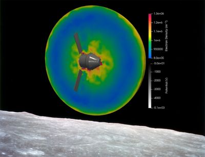
These phenomenological effects are consequences of plasma interactions with ambient fields and are merely approximated in a BEM method, which has limits in its ability to calculate electric fields in relatively low-energy, dense plasmas found in low Earth orbit (LEO) or interplanetary orbits.
However, using PIC and 3D electrodynamic solver technology for surface charging produces predictively accurate simulations of the surface level in any orbit.
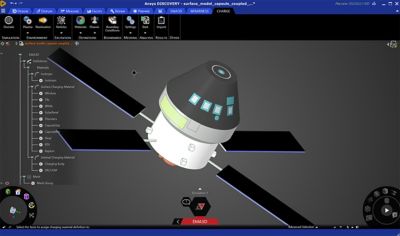
To optimize your simulation further, integration with Ansys Systems Tool Kit (STK) enables you to create a multidomain scenario to visualize your product or project in a realistic mission context.
Simulating Semiconductors Particle by Particle
Plasma enhanced chemical vapor deposition (PE-CVD) and plasma etching are experimental techniques that leverage multiphysics for product development in the semiconductor industry.
PE-CVD explicitly tackles the deposition of material on the surface of a wafer, such as a thin coating. A chemical with free radicals is placed on the surface of the wafer and then the wafer is placed in a plasma chamber. A plasma may be generated from an ambient gas by driving a radio frequency (RF) source. The ions in the plasma interact with the surface of the wafer and the interaction with the radicals create biproducts. The influx of ambient gas and the outflux of biproducts is handled through valves that control the ambient flow of gas.
At this point, various engineering disciplines are needed to properly model the process. Fluid mechanics is needed to model the gas motion in the chamber; electromagnetics is needed to model the RF source and the field interactions with the plasma; plasma physics is required to generate and track the plasma dynamic near the wafer; and chemistry is needed for the interaction of the ions at the surface of the wafer. The PIC solver in EMA3D Charge coupled with its full wave FEM solver and additional Ansys multiphysics simulation tools bridge the gaps throughout the process and effectively connect plasma phenomena with EM physics.
Still, another challenge arises as deposition rates heavily rely on the rate of collision between the ions in the plasma and the surface of the wafer. To tackle this simulation, the PIC models relativistic collisions within a species and between multiple species. The plasma distributions created by the PIC generate EM fields that are captured by the FEM, which is necessary to tackle the production of plasma sheaths that critically contribute to the deposition rates.
To complete the PE-CVD workflow, simply integrate the PIC and FEM solver technology into Ansys Fluent and Ansys Chemkin-Pro to employ computational fluid dynamics (CFD) and chemistry simulation, respectively. The co-simulation between the two solvers will leverage Ansys System Coupling 2.0 to generate a comprehensive simulation
Uniting all Parties and Particles
By engaging PIC solver technology, you experience deep integration at the physics level (coupling EMA3D Charge with Fluent or Chemkin-Pro) and the user interface and workflow level (integrating the software into STK).
EMA3D Charge can also be integrated with Ansys Rocky particle dynamics simulation software or Ansys EMA3D Cable to explore further physics-based simulation. Similarly, to visualize your project in realistic settings as you can in STK, you can employ EMA3D Charge in conjunction with Ansys Discovery 3D simulation software or the Ansys ModelCenter model-based systems engineering (MBSE) platform.
With EMA3D Charge you experience a more comprehensive physics solution with solvers vetted individually, developed and optimized using numerical methods, and paired through System Coupling 2.0. As a result, streamlined workflows accelerate simulation run time from setup to completion.
To learn more, register for the upcoming webinar: EMA3D Foundations and Integrations Part 3: The Particle-in-Cell Solver of EMA3D Charge, scheduled for September 29.
Watch the first and second webinars in the series.
Please note, the original three-part webinar series has been extended with a fourth installment slated for January 2023.