-
-
Access Free Student Software
Ansys empowers the next generation of engineers
Students get free access to world-class simulation software.
-
Connect with Ansys Now!
Design your future
Connect with Ansys to explore how simulation can power your next breakthrough.
Free Trials
Products & Services
Learn
About
Back
Products & Services
Back
Learn
Ansys empowers the next generation of engineers
Students get free access to world-class simulation software.
Back
About
Design your future
Connect with Ansys to explore how simulation can power your next breakthrough.
Free Trials
ANSYS BLOG
June 3, 2021
Solving Chip Designs at the System Level via HFSS 3D Layout
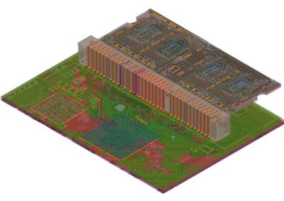
This model of a complex PCB package was generated and solved in just 34 hours using Ansys HFSS 3D Layout. It would take weeks with other approaches.
Semiconductor fabricators are under enormous pressure today to design more powerful chips and printed circuit boards (PCBs) with faster speeds, while mitigating signal integrity issues — all while shrinking the form factor. The result? Massive design complexity, as manufacturers stack more and more components together in ever-closer proximity.
But design complexity isn’t the only issue. Applications in the growing 5G, autonomous vehicle and Internet of Things (IoT) markets are forcing semi manufacturers to not only focus on innovation, but launch their extreme innovations quickly. The current world shortage of chips for automotive applications is just one example of the incredibly demanding and volatile market environment semiconductor fabricators face. Another is Samsung’s recent announcement that it may need to delay the launch of its next Galaxy Note smartphone due to chip availability issues.
Modeling and simulation via Ansys HFSS have helped the world’s semiconductor leaders meet a range of development and launch challenges for decades. Since 1990, Ansys has continuously introduced new functionality and features to anticipate and answer semiconductor customers’ emerging challenges. So it’s not surprising that new capabilities in Ansys HFSS, along with general technology advancements such as cloud computing, support customers’ efforts to design and launch smaller, more powerful, more innovative chips at the speed of demand.
Chief among these advancements is a relatively new capability in HFSS, called 3D Layout, that enables engineers to assemble even the most complex designs, quickly and accurately, at the system level. This is a game-changing development that can help every semi manufacturer compete more effectively and meet market demand, without sacrificing product reliability or confidence, because the gold-standard HFSS solver is being used for the system simulation.
System-Level Simulation: From Vision to Reality
Historically, chip design via Ansys was a sequential, component-level process that was limited by simulation solve times, geometric meshing capabilities, processing speeds and other technology considerations. But today those limitations have been removed — just in time to help semiconductor fabricators achieve a new level of speed by solving even the most complex chip and board designs as an integrated system.
By allowing engineers to model an entire signal path, which would include the integrated circuit (IC) package + connector + board, Ansys HFSS 3D Layout reveals not only component-level design flaws, but any system-level integration or coupling issues such as signal loss between components. Instead of taking a “divide and conquer” approach ― in which different engineering teams design different parts of the signal path from IC to IC in a serial manner, using various tools — semi developers can assemble the full signal path all at once, using a single, industry-standard solution.
Not only is this approach more productive and efficient, because it eliminates hand-offs, but it also equips design teams to identify system-level issues at a very early design stage, when the costs of addressing them are low. In addition, HFSS 3D Layout supports design automation, capitalizing on existing PCB product designs to minimize rework and iterations.
The time and cost savings of HFSS 3D Layout are impressive. Today, engineers only need 34 hours to model a PCB design that incorporates eight two-layer flip-chip BGA packages mounted on a SODIMM board, plugged into a connector that is mounted on a motherboard, with 64 nets and 128 ports. This model would take weeks to generate using a sequential, component-level approach.
How is Ansys able to deliver this revolutionary level of speed and performance? First, Ansys has taken its meshing capabilities, already the gold standard, and dramatically improved their ability to model even the most geometrically complex package quickly and easily. Second, Ansys solvers have been improved to process even the most sophisticated electromagnetic problems in a fraction of the time that was previously required. And finally, Ansys solutions can now access cloud computing resources ― including Ansys Cloud, which runs on Microsoft Azure — to increase the RAM and computing nodes available to solve numerically large problems such as chip design. All of these technology advancements combine to deliver the industry’s fastest, most accurate solve times for full, 3D, system-level models.
The Added Value of a Multiphysics Platform
In addition to the unmatched power, speed, depth and breadth of HFSS 3D Layout, Ansys also offers the industry’s only comprehensive simulation platform for multiphysics PCB and chip simulation. Multiphysics simulation enables semi development teams to accelerate many design steps, as well as test the performance of silicon die, package and board under realistic operating conditions as an integrated system, in a virtual design landscape.
One of the greatest physical challenges for electronics engineers is managing the natural tendency for heat build-up as many components are stacked in close proximity. Beyond thermal effects, semiconductor engineering teams must consider the structural requirements of the overall package, as well as electromagnetic signal and power integrity under real-world conditions.
Ansys delivers an open, extensible and powerful platform that provides easy-to-use, out-of-the-box solutions for multiphysics and multiscale design. The Ansys platform integrates easily with other development tools and data sources, creating a “digital thread” that links siloed development teams and supports true system-level collaboration. By encouraging teamwork and supporting knowledge-sharing, the Ansys platform helps global semiconductor leaders deliver innovation and increase their rate of first-pass system success.
Grab Your Share of the Market Today
While the world’s semiconductor giants are already leveraging Ansys HFSS 3D Layout and the Ansys multiphysics platform to accelerate their design efforts, many small and mid-sized fabricators have yet to discover the benefits of system-level modeling.
Fortunately, Ansys can act as a single source of solutions and expertise to get your organization started in adopting this new industry best practice. Given the growing shortage of chips worldwide, there has never been a better time to accelerate and improve your development efforts. Learn more by watching an on-demand webinar from our HFSS 3D Layout Webinar Series.