-
-
Access Free Student Software
Ansys empowers the next generation of engineers
Students get free access to world-class simulation software.
-
Connect with Ansys Now!
Design your future
Connect with Ansys to explore how simulation can power your next breakthrough.
Free Trials
Products & Services
Learn
About
Back
Products & Services
Back
Learn
Ansys empowers the next generation of engineers
Students get free access to world-class simulation software.
Back
About
Design your future
Connect with Ansys to explore how simulation can power your next breakthrough.
Free Trials
ANSYS BLOG
April 10, 2023
Steps to Minimize IR Drop in Integrated Circuit Design
What is IR Drop?
The potential difference, or voltage drop, between two ends of a conducting wire during current flow is called IR drop (from Ohm’s law: V=IR). In chips, power and ground are distributed through metal networks constituting the power delivery networks (PDNs). When current flows through the PDN, part of the voltage is dropped across the network, as per Ohm’s law. This phenomenon is called IR drop.
This voltage drop in the power delivery network before the voltage reaches standard cell power pins significantly affects the chip's switching speed and performance. The same effect on the ground net leads to ground bounce, in which the nominally zero voltage rises above zero.
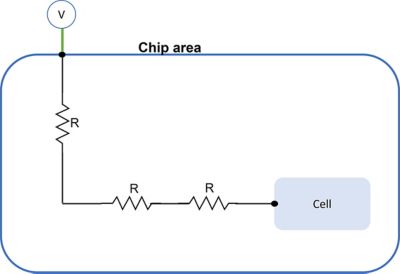
Voltage drop due to parasitic resistance in the interconnect between supply pin and the cell.
As the number of technology nodes goes down, the number of transistors on a chip increases and the wires get smaller. The two major reasons for higher-voltage drop are that chips with hundreds and millions of transistors withdraw a large amount of current through PDNs, and metal wires resist the current flow. Today’s high-performance chips like graphic processing units (GPUs) can easily draw in excess of 200 W, which generates intense supply currents.
Due to IR drop in PDNs, standard cells may not receive sufficient voltage required for their operation, which leads to slower performance. It can even lead to fatal errors in the operation of the IC. The impact of IR drop on circuit timing must be included as an important step in the IC design process to avoid these issues.
Types of IR Drop
The two types of IR drop are static IR drop and dynamic IR drop. Static IR drop happens when the circuit is not functioning and depends on the resistor-capacitor (RC) network of the PDN. Gate channel leakage current is mainly responsible for static IR drop.
When transistors are switching, voltage drop in the PDN is known as dynamic IR drop. More current will be drawn through a PDN when many cells switch simultaneously at a high frequency. This causes fluctuating higher-voltage drop and is known as dynamic IR drop.
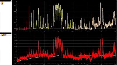
Graph showing time-based power profile.
Best Practices to Minimize IR Drop
PDN Design: The PDN is responsible for distributing power to different parts of the chip, so it's essential to have a well-designed PDN. A well-designed PDN should have low resistance and inductance to reduce voltage drop. The PDN should also have a sufficient number of voltage regulators to ensure all parts of the chip receive the required amount of voltage for their operation.
EMIR analysis by a signoff power integrity tool like Ansys RedHawk-SC can produce build quality metrics (BQM) that measure how well a particular PDN layout meets the power demands of a circuit before placement. Areas of weak power supply can be identified quickly and improved early in the design flow.
Optimizing layout: By increasing the width of metal wires and using fewer vias in the power grid, you can reduce resistance and inductance in a PDN, which in turn reduces IR drop. Optimizing the layout and employing high-speed design guidelines can help reduce voltage drop in PDNs.
Ansys PowerArtist is used to optimize the power delivery network by estimating the power at RTL level.
Proper power and ground plane placement: Power and ground planes in a chip play a crucial role in reducing IR drop for sensitive analog, radio frequency (RF), and mixed-signal designs. Placing power and ground planes close to the transistors reduces the resistance and inductance in a power distribution network. This, in turn, minimizes IR-drop.
Reduce local current demand: Placement algorithms can consider the density of local current drawn by nearby cells and make sure to spread them further apart. This can often significantly improve dynamic voltage drop (DVD) without creating much impact on timing results.
On-chip decoupling capacitors: The use of on-chip decoupling capacitors can help minimize IR drop by providing a low-impedance path for high-frequency noise and reducing the voltage drop. These capacitors should be placed close to the power and ground pins of the transistors. Decoupling capacitors help reduce IR drop by providing a local energy source to the transistors, reducing the need for a large current from the PDN.
IR drop analysis tools: IR drop analysis tools can help you predict and measure IR drop in your chip. These tools can provide a visual representation of voltage drop across different parts of the chip, allowing you to identify root causes for measured voltage drop and pointing to areas that need improvement.
IR drop is a vital signoff validation for taping out any integrated circuits. Reducing it is crucial for ensuring the correct operation of the chip and by following the steps outlined in this blog, you can minimize IR drop and improve the performance of your chip. Check out the Ansys RedHawk-SC and Ansys PowerArtist pages to see how they can help you reduce IR drop.