
ANSYS BLOG
December 15, 2023
The Big Impact of MicroLEDs
MicroLEDs are essentially semiconductor devices that consist of tiny light-emitting diodes (LEDs) with diameters ranging from 5 μm to 100 μm in size, which makes them approximately the same size as a small dust particle or a fine grain of sand.
The Emergence of MicroLEDs
Amid the modern world's incessant hustle, technological advancement has led to devices continuously shrinking, getting faster, and becoming more efficient. Consider the revolution in the world of displays. With the miniaturization of display technologies from liquid crystals to organic light-emitting diodes (OLEDs), displays have come a long way since the days of bulky cathode ray tubes, ushering each new generation with more compact, brighter, and higher-resolution screens. In recent years, microLEDs have emerged as a mighty contender, promising significant improvements in brightness, color gamut, contrast, response time, lifetime, and energy efficiency. From our favorite gadgets and displays in our cars to even high-speed communication networks, microLEDs are promising for a diverse range of applications.
Design Challenges of Miniaturization
For microLED applications, smaller is not only more convenient but also more power-efficient and even less expensive once manufacturing achieves scale. However, miniaturization comes with its own set of challenges. The process of creating such tiny emissive structures results in atomic-level imperfections mostly at the edges of the LED, where current isn’t converted into light and thus reduces the internal efficiency. The smaller the microLED gets, the larger the ratio of its perimeter to its surface area and the more challenging it is to achieve high internal efficiency.
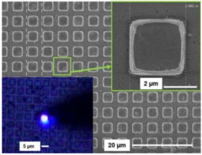
Scanning electron microscope (SEM) micrograph of 3-µm size/5-µm pitch microLED array fabricated with direct bonding approach. Inset: An optical photograph of a microLED switched on. Photo from F. Templier/CEA-SETI
Light extraction and shaping are other key challenges. When you make an LED smaller, the tolerance for changes in dimensions and misalignments becomes more stringent. At the same time, it becomes harder to efficiently extract light from the device while also controlling and avoiding unintended signal or energy transfer between adjacent pixels, known as crosstalk. These challenges become even greater with increasing pixel density.
In addition to the nano-/microscale design of the microLED pixel, designers need to consider the incoherent emission and interaction of large arrays of these pixels at the macroscopic device level. Depending on the use case, there are typically other layers and optical elements such as lenses, filters, color conversion layers, scattering structures, gratings, and polarizers integrated to assist with color definition, beam enhancement, and beam shaping. Combining suitable solvers in seamless workflows for accurate modeling of these building blocks and their interactions is a critical challenge engineers face at the system level.
Now consider the staggering number of microLEDs needed to populate high-resolution display screens — and imagine the daunting task of placing millions of tiny grains of sand with micrometer accuracy. Many manufacturers have been heavily investing in efficient and scalable mass transfer processes for detaching millions of microLED dies from donor wafers, keeping them attached to transfer stamps, then releasing them onto the display substrate in precise locations. Using mass transfer processes and equipment, millions of these microLEDs are transferred to the display backplane and assembled in arrays to form the subpixels within a display. The microLEDs are then electrically connected using metal interconnects to the active complementary metal-oxide semiconductor (CMOS) backplane with the associated switching and driving circuitries. Given shrinking subpixel sizes, solving the problem of creating highly compact, power-efficient, and complex thin film transistor (TFT) drivers that can precisely and quickly control each pixel individually is a major obstacle to overcome.
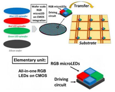
MicroLED smart pixel transfer. Photo by F. Templier/CEA-SETI
Defects can arise at any of the stages throughout a microLED's production life cycle. Consider a 4K display with more than eight million pixels. Even if a fabrication process has a yield of 99.99%, the display can end up with more than 1,000 dead pixels. Identifying and repairing defects at this scale can be very challenging. Thus, methods and technologies for addressing defects and achieving high yields are something to closely watch for.
Key Benefits of MicroLED Technology
MicroLED technology offers several key advantages:
High luminance: Luminance in emissive devices like OLEDs can be increased by raising input current up to a point, after which the device starts to suffer from efficiency rolloff, fast aging, and may require careful thermal management. MicroLEDs can carry large current densities and achieve much higher luminance with high efficiency while maintaining a slimmer profile.
Fast response times: Semiconductor materials used in microLEDs exhibit fast electrical and optical response characteristics, which leads to faster pixel response times compared to the organic materials used in OLEDs.
Independent pixel control: Each pixel in a microLED display can be driven independently to directly control its on and off state, whereas OLEDs rely on organic materials to emit or extinguish light.
Stability and robustness: MicroLEDs are composed of semiconductor materials like gallium nitride (GaN) with superior stability, eliminating the need for complex encapsulation methods. While OLEDs function well in freezing temperatures, high temperatures significantly speed up aging. Thermal management is also challenging in LCDs as it impacts the display’s efficiency, while cold temperatures can result in sluggish performance. The robust underlying LED technology gives microLEDs superior luminance and lifetime for applications facing demanding conditions such as humidity or a wide range of operating temperatures.
What are the Applications of MicroLEDs?
The aforementioned benefits enable microLEDs to excel in specific applications:
Head-up displays (HUDs) and central cluster displays: MicroLEDs' high luminance is critical for driver safety in HUDs and central cluster displays in automobiles and aircraft. Sunlight readability is improved, ensuring that crucial information remains visible under various lighting conditions.
Headlights in automotive lighting: Combined with their high luminance, microLEDs’ ability to selectively control light segments at the pixel level enables precise and real-time control over light distribution and intensity for automotive headlamp applications. The microLED technology has the potential to replace the current micromirrors of digital light processing (DLP) technology in lighting systems and increase the number of controllable light segments in a headlight beyond what was previously possible by DLP. This high pixel count can enable advanced glare-free high-beam headlights for an improved driving experience.
Consumer electronics: Their high luminance and small footprint give microLEDs a key advantage for applications in which information needs to be displayed in a small area while contending with high ambient light like smartwatches and augmented reality (AR) displays, which enhances user experience.
The ability to control each pixel directly combined with their fast response times are especially advantageous in reducing motion blur and ghosting artifacts in applications that require fluid motion rendering and involve fast-moving content such as gaming, sports and action content, and AR/VR.
High-speed light-based communication: Optimizing microLEDs for faster switching times opens the door for their use in high-speed light-based communication applications such as accelerated computing.
Flexible and stretchable displays: The stability and robustness of microLEDs make them a competitive candidate for flexible and stretchable displays, eliminating the need for complex encapsulation methods.
The Challenging and Promising Future of MicroLEDs
Although a few companies like Sony, Samsung, and Konka sell microLED video walls, and other companies have demonstrated various microLED-based prototypes such as luxury TVs and varying sizes of transparent and flexible displays, their widespread adoption has yet to be realized. One challenge is that the barrier to entry has been significantly raised by the well-established and cost-effective OLED technology. OLEDs have enjoyed several decades of significant investment in materials, devices, and manufacturing development that has made them a tenacious rival for TV and smartphone applications.
While achieving differentiation against OLEDs in some applications can be extremely challenging, other applications in which the demanding requirements around high brightness, high-resolution density, response time, power consumption, and robustness in extreme conditions are well suited for microLEDs, are the likely candidates to drive widespread adoption of this technology.
“There’s significant potential for microLEDs in consumer electronics,” says Jose Pozo, Optica’s chief technology officer (CTO). “Technology leaders have knowingly set a precedent of ongoing ‘next-generation’ expectations. Consider how every new iteration of a smartphone comes with the latest enhancements and boasts a better experience. That mindset now applies to any new technology entering the landscape. With wearable technology and augmented and virtual reality relatively nascent fields, microLEDs offer characteristics that make them highly attractive for continued product evolution.” Founded in 1916, Optica a leading organization for scientists, engineers, business professionals, students, and others interested in the optical industry. It is dedicated to promoting the generation, application, archiving, and dissemination of knowledge in the optical field.
There is also ongoing investment in research and development of new materials and techniques that continue to advance the state of OLED technology. Each year new display makers, startups, original equipment manufacturers (OEMs), and equipment makers keep entering the microLED field, and major players in the tech industry continue to pour billions into the development of microLEDs, it is a promising indication that this emerging display technology is fertile ground with significant investment and growth potential.
Additional Resources
To learn more about the simulation capabilities of Ansys Optics for Design of microLEDs, see our application gallery example: MicroLED Multiphysics Design.
See What Ansys Can Do For You
See What Ansys Can Do For You
Contact Us
Contact us today