

ANSYS ADVANTAGE MAGAZINE
DATE: 2019
Speeding 5G Network Infrastructure Design
By Teddy Lee, Signal and Power Integrity Architect for eSilicon, San Jose, U.S.A.

As the world becomes more connected and digital, the need for more data and higher speed is evident. The increase in global internet traffic, along with decentralization of cloud and data centers, has driven wired and wireless networks to support 5G network infrastructures. 5G technology promises to enable 1,000 times more traffic, 10 times faster speed, and a 10 times increase in throughput. These systems are highly complex and push the boundaries of silicon and manufacturing technologies. eSilicon uses Ansys’ chip-package-system modeling and simulation software in a design-and-verification methodology that serves this ever-evolving market with timeliness and precision.
"With design costs in the tens of millions of dollars and re-spins resulting in schedule delays and missed market opportunities, eSilicon relies on Ansys’ chip-package-system (CPS) modeling and simulation software."
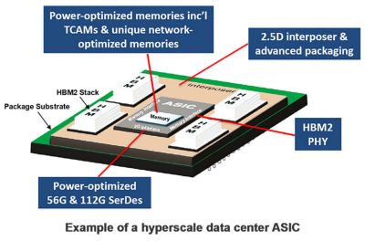
eSilicon’s highly configurable FinFET-class 7nm IP platform includes application-optimized processor core and a number of high-bandwidth memory (HBM) stacks integrated on a silicon interposer, built into a complex 2.5D package.
When designing at the bleeding edge of technology, companies require total system performance, not just chips working to specification. eSilicon addresses these needs with advanced application-specific integrated circuits (ASIC) and intellectual property (IP) for tier-one system original equipment manufacturers (OEMs) in 5G infrastructure, networking, high-performance computing and artificial intelligence markets. eSilicon delivers FinFET ASICs that integrate advanced IP developed by eSilicon at 14nm and 7nm as well as leading-edge 2.5D packaging. This allows the company to deliver lower-power, higher-bandwidth and more flexible products that meet the computational performance and system reliability requirements of customers. As both a developer and a user of advanced IP, eSilicon can deliver a more predictable and robust design.
The complexities associated with smaller semiconductor technology nodes, higher density and tighter margins do increase the risk for system failure during design bring-up or after the product has been out in the market for some time. With design costs in the tens of millions of dollars and re-spins resulting in schedule delays and missed market opportunities, eSilicon relies on Ansys’ chip-package-system (CPS) modeling and simulation software, including Ansys SIwave, RedHawk, HFSS and CMA, to test and validate their design before tapeout. Ansys software models every component across chip, package, substrate and system at a very detailed level and provides an environment that seamlessly integrates each component into a single simulation. Verifying the full system from front to back, as early as possible, is critical to the company’s success. Design methodology that incorporates all the pieces (chip, memory, substrate, package) and ensures that the ASIC works by itself, as well as within the context of the entire system with other uncertainties, lowers risk and shortens time to market.
eSilicon engineers work closely with their customers to manage the complexity of their design and the interfaces. They pay careful attention to the effects of signal integrity (SI) and power integrity (PI) across the chip, package substrate, package and system. Partnering with Ansys, they developed a CPS SI/PI modeling and analysis flow that models every component in a system from die to package to board in detail and simulates all of them together to better understand the impact each component has on the others.
VERIFYING SIGNAL INTEGRITY
As soon as initial layouts for the substrate and silicon interposer are available, eSilicon engineers extract complex 3D structures using Ansys HFSS and Ansys SIwave to generate S-parameter models for insertion loss, return loss and crosstalk performance analyses of high-speed nets. The frequency responses of passive elements are compared to the package specification. Any violations or insufficient margins will result in a design change with additional iterations of extraction and analysis until the requirements are met. For 2.5D package designs, eSilicon engineers connect the substrate and interposer S-parameter models to create a final package model. This model is delivered to the customers to use in an IBIS-AMI channel analysis to verify the transmitter and receiver performance in the time domain.
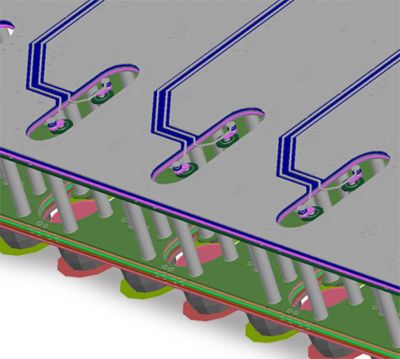
The antipads of the BGA region of the package substrate are enlarged and differentially bridged to reduce capacitance and boost impedance.
Material properties and geometric dimensions of passive interconnects in package substrates can affect the final S-parameter performance. For 2D designs, there are a number of field solvers that can calculate the impedance and SI performance, but the 2.5D packages designed by eSilicon engineers require Ansys HFSS, a true 3D field solver for high-frequency SerDes designs. Inside a package or interposer with dense geometries, nearby structures can have a significant impact on signal performance, especially at high frequencies.
VERIFYING DC POWER INTEGRITY
For DC power integrity, eSilicon engineers model DC voltage drop from the voltage regulator module (VRM) on the board through the trace to the package substrate and silicon interposer. They use Ansys SIwave to extract these components and combine them into a system model. They also use SIwave to run DC simulation for IR/voltage drop, current and power density verification. If any bottlenecks or violations are found, the engineers perform another iteration to improve the power distribution network. By using Ansys tools with high-level accuracy, fast throughput and seamless integration, the engineers are able to improve their design, as well as run quick what-if analyses of design tweaks.
Having an accurate view of the board-to-die power routing, with detailed parasitic extractions at each level, is essential for reliable PI analysis. When engineers assume an idealized voltage regulator module (VRM) on the system board, the simulation results can significantly diverge from real-world performance because localized currents could exceed the average current for the voltage source. Therefore, it is important to define the exact location of the VRM and extract the real traces that will drive the package. By using SIwave, engineers are able to perform a fine-grained analysis of the power distribution network all the way from the VRM to the die ports.
VERIFYING AC POWER INTEGRITY
Managing the impact of noise generated by the die on the system is critical to design success. To have a comprehensive view of power integrity, it is important to understand how power is delivered through the silicon interposer, package substrate and board. eSilicon engineers employ CPS methodology by extracting and modeling each component starting from the die through the interposer, package substrate and PCB. They then simulate the whole system in frequency and time domains. Engineers use Ansys RedHawk to model the die and interposer, Ansys SIwave for the package and PCB analysis, and Ansys CMA for simulation. One of the challenges in verifying the full system with fine-grain accuracy is the varying frequency range of components from VRM to chip.
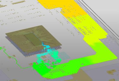
3D model of the voltage plot shows simulated voltage gradients from the VRM to the package, helping eSilicon engineers localize where the drop is happening , such as vias on the PCB, swiss-cheese planes underneath BGA and the package layers.
Simulated voltage gradient from package to chip interface, from BGA balls through substrate vias and finally to the traces leading to C4 interface. Since power distribution network in the package is smaller and denser than the PCB, there is less opportunity for significant IR drop improvement in package design.
Ansys CMA models the full power-delivery network current profile across a wide frequency spectrum of the chip, package and board. It can simulate the large current transients — from a few nanoseconds to milliseconds in duration — in the chip, package and board boundaries that lead to catastrophic global rail voltage collapse.
The goal of AC power integrity analysis is to ensure acceptable transient supply noise by optimizing impedance. If supply noise is too high or its margin is too low, the engineers will loop back to the frequency domain for more decap optimization, or even further back to the layout. By performing analysis early in the design phase, eSilicon engineers are able to optimize the performance instead of simply verifying it.
FREQUENCY DOMAIN SELF-IMPEDANCE AND CAPACITOR OPTIMIZATION
As part of the frequency-domain analysis, eSilicon engineers observe the self-impedance from the die and its effects on each component in the system. They need to determine if any package-level capacitors are needed to lower system-level resonance at the package. Using Ansys SIwave, they calculate target impedance and detune the resonance frequencies by adding different capacitor values and quantities.
TIME-DOMAIN SIMULATION
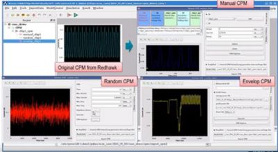
Once decaps are optimized in the frequency domain, eSilicon engineers perform time-domain simulation to analyze the power-supply noise at the die. They use Ansys RedHawk to generate the current profile and extract an electrical model of the die’s power delivery network. RedHawk is primarily a die-level tool, so simulation produces a current profile with high-frequency data but only for a very short duration. However, a longer period is required for the lower bandwidth in system-level analysis. Extending the current profile is not as simple as repeating the waveform, since current modulation is used to excite specific resonant frequencies or to model some functional mode such as TCAM memory access. Ansys CMA allows eSilicon engineers to modulate the current profile to any envelope and output frequency domain impedance, as well as any time domain transient noise. In addition, Ansys CMA automatically connects complex interfaces between the die, interposer and package, which saves a significant amount of manual effort and reduces the risk of error.
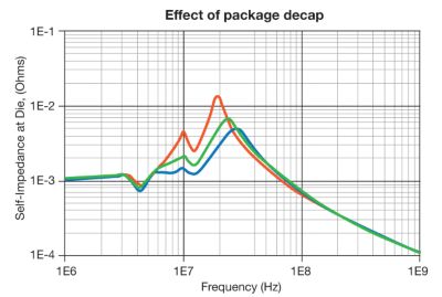
Observation of the effect of adding more 1 uF capacitors at the package level. Increase in quantity showed lower impedance at the parallel resonance. Once target impedance was reached, further optimization focused on effectiveness of mixes of capacitor values and quantities.
Once the extended and modulated current stimulus is available, eSilicon engineers analyze the entire power-distribution network using time-domain simulation with Ansys CMA. They compare simulation results against the allowable noise specification to see if there are any violations. If additional margin is needed, the engineers will go back to frequency-domain simulation to further optimize the design by changing capacitance on the die, package or board; they may even go back further in the design process to optimize the layout of the power distribution network.
eSilicon services tier-one system OEMs whose challenges go beyond lower power, higher performance and smaller size. They are concerned about lifetime performance, thermal and mechanical reliability, and integration with firmware and software. With the level of complexity involved in getting this scale of project to market, design and verification methodology around CPS flow using Ansys’ suite of tools helps eSilicon to accelerate time-to-profit.
References
Erfahren Sie, wie Ansys Ihnen helfen kann
Erfahren Sie, wie Ansys Ihnen helfen kann
Contact Us
Kontakt