
ANSYS BLOG
October 27, 2023
What is a Metalens and How Do They Work?
Metalenses (and more general metasurfaces) are increasingly seen as viable solutions for improving system performance while reducing system size and weight in complex imaging and illumination devices. This is because a single metalens can often be used to achieve the same performance that would otherwise require multiple “traditional” optical components within the device.
However, designing metalenses that can meet system requirements and be manufactured at scale remains a significant challenge. This is in part because metalenses can range in diameter from hundreds of microns — when they are being deployed in compact devices such as image sensors and endoscopes — to centimeters (or larger) when they are being used to replace thicker refractive components in systems such as cellphone cameras or augmented reality (AR) headsets.
Robust metalens design requires multiscale, multiphysics simulation that can provide an accurate assessment of both the lens performance across this wide range of apertures and the performance of the metalens inside of a larger optical system.
What is a Metalens?
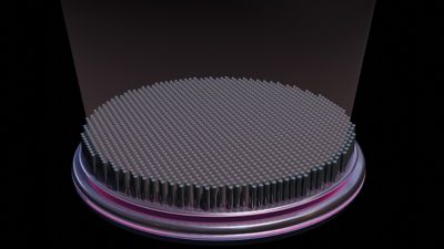
A metalens employs a subwavelength “meta-atom” pattern on a dielectric surface to manipulate incident light. Specifically, the meta-atom pattern modifies the phase profile of the incident light beam, causing the beam to be bent (redirected). Meta-atoms are tiny, nanoscale structures with varying shapes and sizes whose position across the lens can be arbitrary and are designed to control the interaction of light. While the “lens” in metalens implies these components are used for focusing light like a traditional lens, the term has been adopted by the industry to cover a wide range of functionalities that phase manipulation affords.
To achieve this phase manipulation, metalenses require a large difference between the index of refraction of the meta-atoms and that of the surrounding material. The materials used for metalenses depend on the target wavelength range for the application of interest, in which material absorption is minimal and fabrication technologies can meet the feature size demands. For example, silicon is generally considered for near-infrared (IR) applications like lidar sensors, whereas titanium dioxide, gallium nitride, and silicon nitride are considered for camera applications in the visible wavelength range.
How are Metalenses Manufactured?
The method of fabrication will determine the possible meta-atom patterns that can be employed in a metalens design. Current fabrication methods include:
- E-beam lithography, which employs a focused beam of electrons to create nanoscale patterns on a substrate, offering exceptional precision and versatility in nanofactrication. This method is primarily for research applications, as it is not appropriate for mass production of metalenses.
- DUV lithography, which utilizes deep ultraviolet (DUV) light to transfer intricate patterns onto a photosensitive material. This makes it a crucial technology in semiconductor manufacturing for high-resolution patterning.
- Nanoimprint lithography, which involves pressing a mold with predefined nanostructures onto a substrate. This provides a cost-effective and scalable method for replicating nanoscale patterns with high precision.
All the above methods support flexible definitions of the meta-atom pattern in the XY plane of the surface, but they have limited ability to support variations in the Z direction. Therefore, many current metalens designs are based on binary shapes, in which the meta-atom pattern is uniform in Z but arbitrary in the XY plane.
The method of fabrication also influences the choice of materials for metalenses. For example, lithographic fabrication is amenable to the use of silicon or other materials that are already used frequently in semiconductor manufacturing. Nanoimprint lithography also uses different types of UV or thermal-cured epoxies.
All in all, metalenses present challenges for manufacturing at scale for low cost, as they combine small feature sizes (for phase manipulation) with large footprints (for numerical aperture/beam size). We are still in the early days of metalens manufacturing, and thus it is not clear whether some material systems or fabrication processes will provide the economy of scale enjoyed by the semiconductor and photonic integrated circuit (PIC) industries. However, in some application spaces, the benefit of using a thin metalens over traditional optics may outweigh its cost, particularly when compared to the system cost for sophisticated technologies such as a medical endoscope.
What are the Benefits of Metalenses?
The metalens is a flat, lightweight option that can replace bulky traditional lenses and other components in optical systems. A single thin metalens can combine the functionality of multiple optical components in a complex system — for example, replacing the mask and lens system used in a traditional dot projector. Metalenses can also be used to achieve additional functionalities like polarization manipulation and splitting. In fact, polarization is being leveraged to combine functionalities in sources such as dot projectors and diffusers for 3D sensing in applications like AR and computational photography.
What are the Applications of Metalenses?
Metalenses can be employed in any case in which it is important to reduce the size and weight of the optics in the system. These include lidar for 3D sensing in autonomous vehicles and facial recognition systems; medical devices such as endoscopes and microscopes; surveillance systems such as IR and machine vision cameras; display and imaging systems such as cellphone cameras, CMOS image sensors, and AR/VR headsets; and holography.
The Future of Metalens Technology
In the chip-making industry, a collection of essential tools, libraries, and data used by designers to create integrated circuits within a specific manufacturing process are pulled together in what is commonly known as a process design kit (PDK). As metalens manufacturing continues to mature, we can expect to see PDKs emerging, just as we see in the semiconductor and PIC industries. PDKs allow metalens designers to work with proprietary and verified meta-atom structures offered by foundries, keeping the designer’s focus on the application as opposed to the subwavelength design. As such, foundries play an important role in the metalens ecosystem, which also includes metalens manufacturing companies and fabless design companies. Partnerships within this ecosystem will be very important as designers start looking for libraries of meta-atoms that they can readily use to design their complex metalenses.
In this manner, PDKs represent “black box” building blocks for metalens design. However, they need to be accompanied by design and simulation tools that explore manufacturability through yield analysis and tolerancing. As each manufacturing run is costly both in terms of money and time, these types of analyses are crucial to reducing the number of runs by developing sufficiently robust designs.
The Role of Simulation in Metalens Design
Metalenses are complex optical components whose impact on system performance cannot be assessed without simulation. Simulation enables rapid design decisions by supporting design optimization, tolerancing, and yield analysis. But the efficient simulation of a centimeter-size metalens containing nanometer-size meta-atoms — and the subsequent simulation of that metalens inside of an optical system that may be tens, hundreds, or thousands of centimeters in size — is no small feat. Simulation tools need to be fast, accurate, and robust, as well as multiscale and multiphysics in nature.
Within a metalens, the meta-atom size and shape vary smoothly with position to focus light incident on the lens. This smooth variation allows metalenses to be simulated using efficient algorithms like rigorous coupled wave analysis (RCWA). The results from RCWA modeling of a metalens can then be directly used inside tools for simulation of the full optical system, either using Fourier propagation or geometric ray tracing.
Integrating the metalens model into the full system simulation is critical to the design process. Only by doing so can the designer understand how the metalens will function inside the system and whether this component will enable the system to achieve the required performance within the desired size and weight. As metalenses become integrated into full systems, it also becomes increasingly important to model the impacts of mechanical stress and thermal loading on both the performance of the metalens and the full optical system.
The design workflow for metalens-enhanced optical systems follows several steps that are supported by streamlined data exchange interfaces between Ansys Optics tools. Read the details of this workflow for both small-scale and large-scale metalenses to learn more. Note that for large-scale metalenses, the system may include tens of billions of meta-atoms, so a critical piece of the workflow is the efficient export of the metalens structure to GDS format for manufacture.
The metalens represents advanced, innovative technology that has the potential to transform optical design for a wide range of applications and industries. Their design and fabrication are both complicated and challenging. Even more challenging is understanding how metalenses will behave inside of the optical systems they are meant to enable. As manufacturing methods evolve, simulation will need to keep pace. A robust multiscale and multiphysics simulation architecture is therefore essential to the design of current and future metalenses.
Simulation is the superpower that will unlock our ability to leverage this advanced technology for years to come.
See What Ansys Can Do For You
See What Ansys Can Do For You
Contact Us
Contact us today